

In the world of high-performance computing, Quality Engineering has traditionally been divided into silos. There are the Physical Engineers who inspect solder joints and cable crimps using standards like IPC-610/620, and there are the Signal Integrity Engineers who analyze digital error rates and waveforms. But with the arrival of AI clusters like the NVIDIA NVL72, those silos are collapsing. A microscopic defect in a solder joint is no longer just a ‘workmanship’ issue, it’s a data center outage waiting to happen.
My goal is to build a ‘Full Stack’ Interconnect profile: the ability to trace a system-level failure (like an InfiniBand link drop) all the way down to the physics of a single solder joint. This week, I bridged a critical gap in that stack by analyzing how Solder Reflow, a standard manufacturing process, can quietly destroy the performance of high-speed connectors.
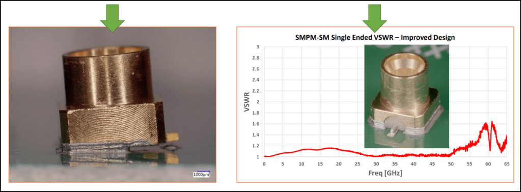
In this Webinar, the speaker talks about thick gold plating which caused wetting imbalance during reflow, leading to “Tombstoning” issue (components lifting up). To address this issue, the internal contact had several design changes to improve the VSWR variation (Voltage Standing Wave Radio).
For ease of understanding, consider VSWR as a Echo meter. When you send a signal down a line, you want 100% of it to go to the receiver. If there is a “bump” (Impedance Mismatch), some signal bounces back. The score 1.0 means – Perfect. No echo. All signal goes through. A score of 3.0+ means Bad. A huge amount of signal is bouncing back. The link will likely fail.
This proves that for connectors like Mirror Mezz or MCIO, controlling the solder volume (wicking) and internal geometry (swept contacts) is the only way to guarantee stable performance vs. random link failures
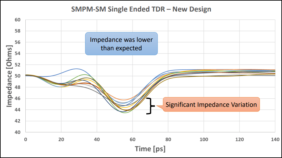
This below chart is an X-Ray of the manufacturing consistency. The X-Axis is distance into the connector. The ‘Dip’ at 60ps shows that on some units, solder wicked up the pin, adding capacitance and dragging the impedance down from the ideal 50 ohms. The spread of the lines proves the reflow process was out of control.”
To solve impedance variation, they attacked the problem from the Connector, the PCB/Stencil, and the Process itself.
- Changing the Connector (Geometry Fixes)
- Added a Solder Control Tail: This acted as a barrier or dam, physically stopping the solder from wicking further up the pin. This minimized the “capacitive stub” effect.
- Added a Chamfer: This created a designated “pocket” or space for excess solder to pool harmlessly. Instead of flowing into critical signal areas, the solder filled this chamfer, preventing the “hidden pooling” issue.
- Changing the PCB / Stencil (Volume Control)
- Stencil Aperture Modification: This kept the solder paste further away from the critical inner areas of the connector. By forcing the solder to start further back, they prevented it from migrating/wicking into the “danger zone” during reflow.
- Thinner Stencil: This reduced the total volume of solder available, lowering the risk of excess solder causing wicking or pooling.
- Changing Process Factors (Thermal & Chemical)
- Moderate Reflow Profile: Lower heat reduces the energy that drives the solder to wick up the pin.
- Solder Paste & Environment: They switched from “Water-Soluble” paste in Nitrogen to “No-Clean” paste in Air.
By implementing these changes, they successfully reduced impedance variation and increased the usable bandwidth of the connector from <25 GHz to >55 GHz
Key Takeaways from the Webinar
I summarized this chapter in my own words and let AI assess my understanding, I was able to get 95% correct. However, I had some questions remained. When reviewing the TDR graph, how did the speakers knew it was an issue related to solder wicking and not just contamination or wires getting crushed. So here is the simple explanation:
The TDR graph alone cannot tell us “This is Solder” vs. “This is a piece of metal shaving.” It only tells you the Electrical Nature of the defect. Here is how to differentiate them from SQE lenses:
Clue 1: The Direction of the Spike (Capacitive vs. Inductive)
- The Dip (Downwards): Means the area became Capacitive (electrically “fat”). The usual suspects are : Solder wicking (adding metal), water intrusion (high dielectric constant), or crushed dielectric.
- The Peak (Upwards): Means the area became Inductive (electrically “thin” or broken). Cold solder joint (gap), broken pin, dirt/contamination preventing contact, or a trace etched too thin.
In this Webinar: The chart showed a Dip. This ruled out “broken parts” or “contamination” (which often causes opens/peaks) and pointed immediately to “extra metal” (Solder).
Clue 2: The Exact Location (Time = Distance)
- We know the connector is soldered at the “Launch.”
- If the TDR shows the dip exactly at 60ps (the Launch point), we know the issue is related to the attachment process.
- If the dip was at 200ps (down the cable), we would know it’s a cable crushing issue, not a reflow issue.
Clue 3: The “Twin” Verification (Simulation & Cross-Section)
This is exactly what the speakers did to prove it was solder and not something else:
- The TDR said: “Something Capacitive (Dip) is happening at the Launch (60ps)”.
- The Physical Lab said: They cut the part open (Cross-Section) and saw the solder wicking.
- The Simulation said: They modeled “Solder Wicking” in software, and the simulation graph matched the real-world TDR graph perfectly.
So as an SQE, We don’t just “guess” its a solder issue.
- The TDR tells me Where (Launch) and What type (Capacitive/Inductive dip)
- Process knowledge tells likely suspects (Reflow adds material -> Capacitance)
- Cross sectioning (destructive) confirms the root cause.
Final Thoughts
The presenter mentions that the Reflow/Impedance issues discussed are not limited to just Surface Mount (SM) connectors; they also plague other types of connectors as well. So going forward, my supplier audits won’t just ask, ‘Did the solder joint pass visual inspection?’
I will now ask: ‘How have you validated your reflow profile against the impedance requirements of the connector?’ and ‘Show me the TDR data that proves your solder volume isn’t creating a capacitive stub.’
This is the difference between inspecting for ‘Compliance’ and inspecting for ‘Performance.’ Next up, I’ll be diving into Teledyne LeCroy’s High-Speed Characterization series to learn exactly how to measure these invisible defects myself.
